1Institute for Biomedical Engineering, ETH Zurich and University of Zurich, Zürich, Switzerland
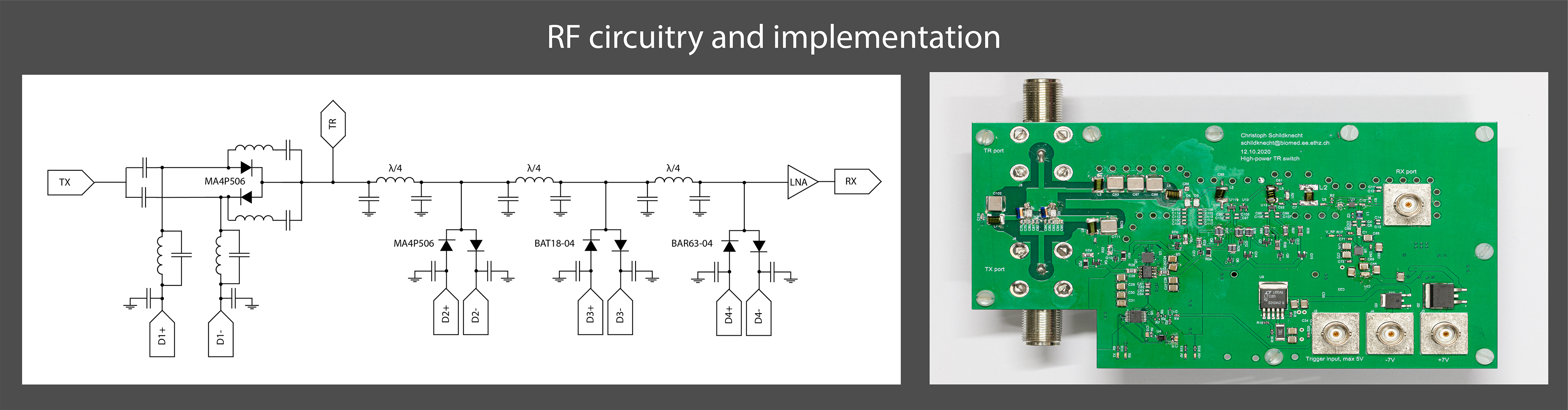
Left: Illustration of the RF topology of the high-power T/R switch. The antiparallel PIN diode pairs are driven in a cascaded way. Towards the RX port, PIN diodes with shorter carrier lifetime are deployed.
Right: Implementation of such an RF topology. In addition, auxiliary circuits and low noise amplifier (LNA) can be seen.
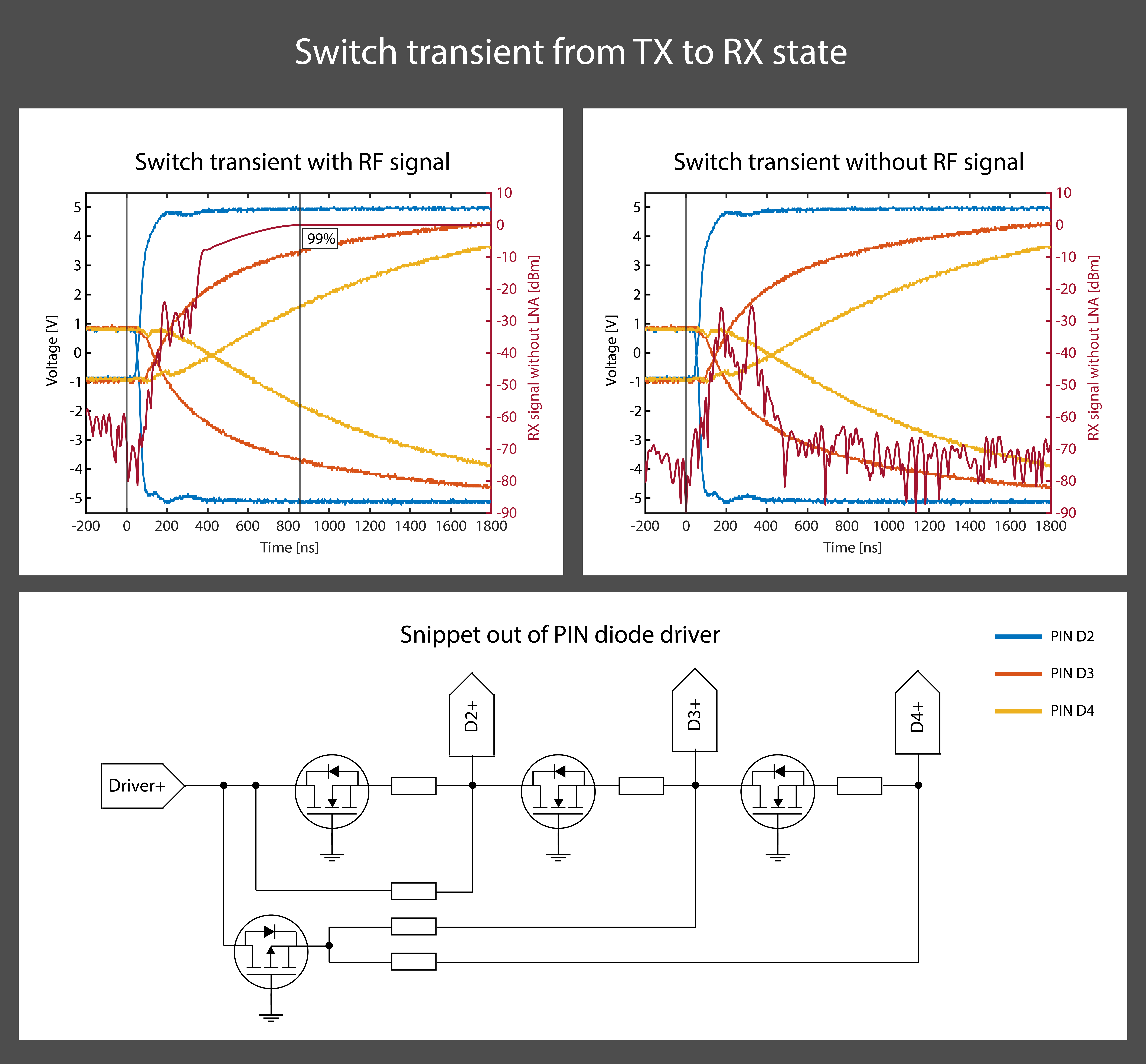
Top row: transient switch behavior when switching from the TX to the RX state. The reverse bias is built up in a cascade, which reduces the transient voltage peaks.
Bottom row: Snippet out of the passive self-triggered PIN diode driver. As long as a PIN diode is still in its low impedance state, it has a forward voltage present, despite bulling a reverse current out of it. When the PIN diode changes to its high impedance state, current is drawn out of the next stage.